


World Class Infrastructure
The World Class Facilities and Infrastructure service provides industry and research partners with access to comprehensive testing, analysis, and validation capabilities essential for semiconductor and electronics development. These shared facilities are designed to support the full product lifecycle, from early development and debugging to reliability qualification and failure investigation.
Role and Function
This service enables organizations to conduct advanced testing and analysis activities without the need for heavy capital investment, while ensuring compliance with industry standards and best practices.

Electrical Testing Capabilities
- Wafer probing and electrical characterization for device performance evaluation
- Logic analyzer testing for functional verification and signal integrity analysis
- Curve tracer measurements for device behavior and parameter extraction
Frequently asked questions
This section provides concise answers to common questions regarding our failure analysis and reliability testing capabilities, the value we deliver to the industry, and the industries we serve. For further information or specific inquiries, please contact our team.
1. What failure analysis capabilities are available?
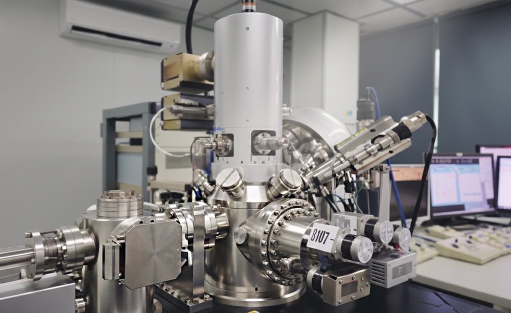
The facility offers comprehensive failure analysis services, including optical microscopy for initial inspection and defect localization, Scanning Electron Microscopy (SEM) for high-resolution structural analysis, Energy Dispersive X-ray (EDX) for material composition identification, and X-ray inspection for non-destructive internal failure investigation.
2. What reliability testing analysis capabilities are provided?
Reliability testing includes High Temperature Operating Life (HTOL) testing for long-term reliability assessment, temperature cycling tests to evaluate thermal stress endurance, and burn-in testing to detect early-life failures.
3. What value does this provide to the industry?
These services help improve product quality and reliability, enable early detection of design and process issues, and offer cost-effective access to advanced testing infrastructure.
4. Which industries are served?
The services cater to semiconductor manufacturing and design, electronics manufacturing services, as well as research and development organizations.